

MIT engineers have developed a new technology for creating semiconductor transistors that are only a few atoms thick, paving the way for more powerful and energy-efficient computer chips. In this article, we will explore the new technology in detail and discuss its potential implications for the world of electronics.
Introduction:
Over the years, the semiconductor industry has undergone a rapid transformation, leading to the development of smaller, faster, and more energy-efficient computer chips. These chips power a wide range of electronic devices, from smartphones and laptops to cars and smart homes. However, as the demand for faster and more powerful computing devices continues to grow, the industry faces new challenges in designing more efficient chips.
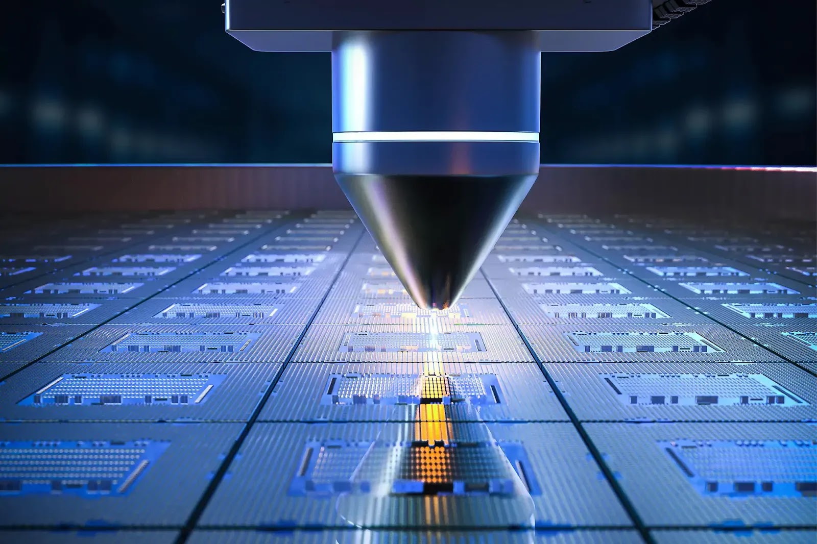
MIT engineers have made a significant breakthrough by developing a new technology that could help create more powerful and denser computer chips. They have developed a new type of semiconductor transistor that is only a few atoms thick, making it an incredibly efficient and compact component for electronic devices.
The Technology:
The new technology developed by MIT engineers uses a special type of semiconductor material known as a transition metal dichalcogenide (TMD). This material is just a few atoms thick and is known for its excellent electrical properties.
Also Read:- The Deadly Effects of Air Pollution on Human Health
- 2024 Mercedes-Benz E-Class: A Game-Changer Among Luxury Wagons
To create the transistor, the researchers placed a small piece of TMD on top of a substrate made of silicon dioxide. They then used a technique known as chemical vapor deposition to grow additional layers of the material on top of the initial layer.
The resulting structure consists of a thin layer of TMD sandwiched between two layers of silicon dioxide. The TMD layer acts as the channel through which electrons flow, while the silicon dioxide layers act as insulators, preventing the electrons from leaking out.
Advantages of the Technology:
The new transistor technology developed by MIT engineers offers several advantages over conventional semiconductor transistors. First and foremost, the technology allows for the creation of incredibly small and efficient transistors. Since the transistors are only a few atoms thick, they take up very little space, allowing for the creation of more compact and powerful computer chips.
Secondly, the new technology could also help reduce the energy consumption of electronic devices. Since the transistors are so small, they require very little power to switch on and off, reducing the overall power consumption of the device.
Finally, the technology is also incredibly scalable, allowing for the creation of larger and more complex integrated circuits. This means that the technology could be used to create more powerful and energy-efficient processors for a wide range of applications, from smartphones to data centers.
Potential Applications:
The new technology developed by MIT engineers could have a wide range of applications in the world of electronics. It could be used to create more powerful and energy-efficient computer processors, leading to faster and more efficient computing devices.
It could also be used to create more efficient solar cells, as the thin TMD layer could be used to capture more light, increasing the overall efficiency of the cell.
Additionally, the technology could be used in the development of more sensitive sensors for a wide range of applications, from healthcare to environmental monitoring.
So, the new semiconductor transistor technology developed by MIT engineers represents a significant breakthrough in the field of electronics. It offers several advantages over conventional transistor technology, including increased efficiency, smaller size, and scalability.
The technology has the potential to revolutionize the semiconductor industry by enabling the creation of more powerful and energy-efficient computer chips. It could also have a wide range of applications in other fields, including solar energy and sensor technology.
Read More:- Redfall: A Game That Pushes the Limits of PC Gaming with Nvidia GeForce RTX
- The Rise of E-Ink Displays: Innovative Uses and Open-Source Options
That's it for this article.
Thanks for Visiting Us – Fixyanet.com


0 Comments